Crystallographic Stargate
© 2015 Stefano Vespucci
When electrons interact with materials, beautiful patterns may be produced. Our image is an artistic view of a pattern produced from a silicon crystal when electrons reflected from the surface and the bulk of the crystal interact. Such patterns allow the separation of the atoms of the crystal to be determined. These measurements are vital for understanding the properties of new synthesised materials ranging from metal alloys to semiconductors.
Research by Stefano Vespucci from Strathclyde Physics
Research by Stefano Vespucci from Strathclyde Physics
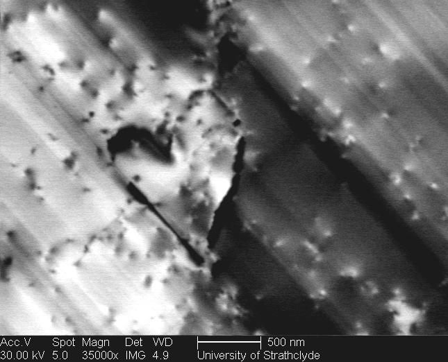
Baby Blue Blanket

© 2013 Nouf Allehiani
Light emitting diodes (LEDs) are not only an energy-efficient light source that could replace conventional light bulbs, they also have medical applications. For instance blankets incorporating blue LEDs are used for the treatment of jaundiced infants. My PhD work is to characterize nitride semiconductors which can emit light from the red to the ultra-violet. In order to develop high brightness and efficient LEDs, we investigate the role of defects that affect the light emission. The presented image is an electron channelling contrast image from an AlGaN thin-film revealing defects (black dots) and atomic steps (dark lines).
Research by Nouf Allehiani from Strathclyde Physics in collaboration with Technische Universitat Berlin
Research by Nouf Allehiani from Strathclyde Physics in collaboration with Technische Universitat Berlin
Dislocations Discotheque
© 2012 Naresh Kumar & Mark Burns
The availability of a simple, non-destructive technique to rapidly detect and identify defects in semiconductors would represent a real step forward for the development of new devices such as UV LEDs, high power green laser diodes, high power transistors and potentially, semiconductor-based ferromagnets. Such devices have applications as diverse as air and water purification, lighting, data processing, data storage and energy conservation and distribution. Recently we have developed a method which allows the unambiguous identification of the most common defects in semiconductors (e.g., GaN, ZnO and SiC), namely threading dislocations. This new method reduces the time required to obtain quantitative and statistically significant information on dislocations compared to presently available techniques. The presented image is a scanning electron microscope – electron channeling contrast image acquired from a GaN thin film showing individual dislocations and atomic steps. An artistic impression of the channeling electrons has been generated by combining displacement mapping, three dimensional rendering and two dimensional compositing techniques.
Research by Naresh Kumar from Strathclyde Physics; visual effects by Mark Burns from City of Glasgow College
Research by Naresh Kumar from Strathclyde Physics; visual effects by Mark Burns from City of Glasgow College
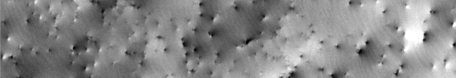
Stacking Fault in a Nano Heart
© 2011 Naresh Kumar
The displayed image is an electron channeling contrast image (obtained using a scanning electron microscope) of a non polar GaN thin film for optoelectronic applications. The black and white contrast features (dots) are threading dislocations. The dislocations together with stacking faults have assembled to form a heart shaped nano-feature.
Research by Naresh Kumar from Strathclyde Physics
Research by Naresh Kumar from Strathclyde Physics