(Funding available for European/UK students)
3-D nanoscale structural analysis of materials in the scanning electron microscope through application of direct electron detectors
The PhD student will join our multidisciplinary research team developing and applying novel scanning electron microscopy techniques to the understanding of materials.
See https://gan-sem.phys.strath.ac.uk/ for some of our current research activities.
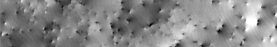
This project is focussed on developing and applying next generation detectors for the scanning electron microscopy techniques of electron backscatter diffraction (EBSD) and electron channelling contrast imaging (ECCI). The unique properties of our detectors will enable the investigation of the structural properties of materials on the nanoscale, enabling for example the investigation of defects in single nanorods.
This joint project between The University of Strathclyde, Glasgow and the National Physical Laboratory, Teddington also promises to open up a whole new research area in non-destructive three dimensional texture, strain and defect mapping in solid-state materials. Such information is invaluable for the optimisation of new materials ranging from steels for the automotive industry; to titanium based alloys for aerospace applications; to semiconductor thin films for use in the solid state lighting and electronics industries.
The student will work together with researchers at The University of Strathclyde, the National Physical Laboratory, the University of Glasgow and other research collaborators from both academia and industry. The project is to interface a direct electron detector to a dual beam (electron and ion beam) instrument for three-dimensional analysis of the structural properties of materials via the novel scanning electron microscopy techniques of EBSD and ECCI. The use of such a detector will dramatically improve speed and performance of such measurements. Materials problems to be addressed include the optimisation of ion implantation in semiconductors – this will also take advantage of the new electron probe microanalyser to be installed within the new Technology and Innovation Centre at the University of Strathclyde. We will also exploit the unique properties of our new detectors to probe the structural properties of thin film and nanopatterned semiconductor electronic and opto-electronic device structures.
The student will be based at the University of Strathclyde but will have the opportunity to spend substantial time at the National Physical Laboratory.
To discuss the project please contact Dr Carol Trager-Cowan: c.trager-cowan@strath.ac.uk
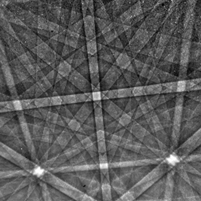
Diamond EBSD pattern
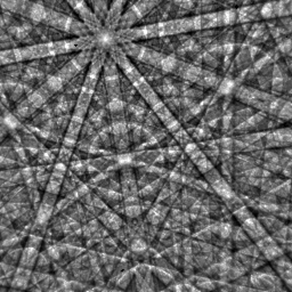
Gallium nitride EBSD pattern