© 2013 Nouf Allehiani
The aim of this project is to produce a step change in the performance of the scanning electron microscopy techniques of electron backscatter diffraction (EBSD), and electron channelling contrast imaging (ECCI), and exploit these relatively new techniques together with cathodoluminescence imaging (CL) and electron beam induced current (EBIC) for the characterisation and hence the improvement of nitride semiconductor thin films. Such materials are used in the manufacture of UV/blue laser diodes, UV/visible LEDs and white LEDs. Nitride laser diodes are presently dictating the development of next generation DVDs and developments in printing and colour copying. Present applications of nitride LEDs extend from street lighting, to back lighting in mobile phones, to traffic lights. Future use of nitride-based LEDs promises to revolutionise lighting in the home and office. Nitrides are also being developed for the production of high frequency, high power electronic devices.

© 2012 Naresh Kumar & Mark Burns
EBSD is an attractive technique with which to interrogate the crystallographic properties of materials because it can provide information on crystal orientation, polytype and strain with a resolution of tens of nanometres. In EBSD an electron beam is incident on a sample which is tilted at an angle of typically 70°. The impinging electrons are scattered inelastically through high angles forming a diverging source of electrons that can be diffracted. A simple description for the formation of an electron backscatter diffraction pattern (EBSP) presumes that electrons that satisfy the Bragg condition for a given plane emanate in diffraction cones from both the upper and lower surfaces of that plane. When these cones intersect a phosphor screen Kikuchi lines are observed. An EBSP consists of a large number of overlapping Kikuchi bands and is a 2-D projection of the crystal structure. Rotation of a crystal will produce a rotation of the EBSP; a tilt of a crystal will produce a shift in the EBSP, strain will produce distortion of the EBSP. EBSPs acquired from a mesh of points on a sample will produce a map of tilt, rotations or strain in that sample. In the course of our research we aim to attain much improved levels of sensitivity (less than 1 part in 10,000) to changes in tilt, rotation and strain to obtain detailed high resolution information on the crystallographic texture and strain distribution in nitride semiconductors.
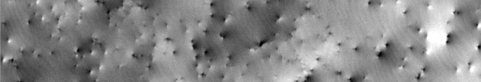
ECCI can be used to reveal single crystallographic defects such as dislocations in semiconductor thin films. In ECCI the intensity of electrons backscattered from a suitably oriented sample depends on the relative orientation of planes in a crystal. Changes in crystallographic orientation or changes in lattice constant due to strain are revealed by changes in grey scale of an image constructed by monitoring the intensity of backscattered electrons as an electron beam is scanned over the sample. Defects are imaged due to lattice plane tilting and strain they produce. Our aim is develop the ECCI technique so that it may be used to fully characterise all defects present in our films.
We plan to apply these powerful techniques to optimise the quality of nitride semiconductor thin films, including:
- non-polar and semi-polar nitride thin films
- epitaxially overgrown nitride thin films and nitride thin films grown on native substrates
- high aluminium content nitride thin films (including films grown on silicon)
- high indium content nitride thin films
- zinc blende nitride thin films
Such novel nitride semiconductor structures will allow the production of higher power LEDs and extend their wavelength range to the red and infrared. They will also open up new applications for nitride-based devices – solar cells for example.
Throughout the project we will also establish with industrial partners the best routes for development and commercialisation of new instrumentation, and nitride thin film growth processes.