In the development and study of new materials, the understanding of their crystal structure plays a crucial rule. Electron backscatter diffraction (EBSD), also known as backscatter Kikuchi diffraction (BKD), is a technique used to obtain accurate crystallographic information from bulk materials, thin films and nanostructures with high spatial resolution [1] (of order 20 nm). Typical materials which can be investigated by EBSD include metals, rocks, ceramics and semiconductors. The technique allows the identification of individual grain orientations, grain boundaries and phase identification [1, 2]. It is also used to study processes like recrystallization and grain growth, and it is a very powerful tool in the study of strain fields in crystals [3].
EBSD patterns were first observed by Nishikawa and Kikuchi in 1928, in both backscattering and transmission modes, using electron-sensitive film [4]. The technique was developed further by Alam et al in the 1950s [5], and later by Venables and Harland (1973) and by Venables and Bin-Jaya (1977) [6, 7]. In 1984 the first commercial system was produced by Moon and Harris, exploiting the work of Dingley at the University of Bristol [8]. In the 1990s fully automated EBSD systems in the SEM had been developed by Adams et al [9] and Krieger Lassen et al [10, 11]. The capability to automatically index EBSPs and map the spatial distribution of crystal orientation led to EBSD becoming a good alternative to X-ray pole figure analysis of texture, and so opened up new horizons in quantitative orientation mapping and grain boundary studies [1].
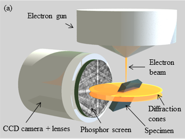
Figure 1: Illustration of the EBSD detection geometry and a conventional EBSD detector.
Experimentally, EBSD is conducted in a scanning electron microscope (SEM) equipped with an EBSD detector. Commercial EBSD detectors consist of an electron sensitive screen (a phosphor or a scintillator) placed in front of the specimen which is usually tilted by approximately 70° to the normal of the exciting electron beam. A digital camera is used to acquire an image of the diffraction pattern formed by the backscattered electrons impinging on the screen [1, 12]; this is illustrated in Figure 1.
An electron backscatter diffraction pattern (EBSP) is shown in Fig. 1 (b). A detailed description of the intensities in EBSPs is possible using a Bloch wave approach to the dynamical theory of electron diffraction [13, 14]; however, the geometry of the EBSP can be described, to a first approximation, by considering the angular position of electrons which have been Bragg reflected from the lattice planes of the crystal specimen. On penetrating the specimen, the electrons of the impinging beam are both elastically and inelastically scattered. This creates a diverging source of electrons with a broad range of energies [2, 15, 16, 17, 18, 19, 20, 21]. The elastically scattered electrons and quasi-elastically scattered electrons (those electrons which have lost only a relatively small amount of energy through phonon or plasmon scattering) may travel in such a way that their energy and direction satisfy the Bragg condition, $2d\sin{\theta} = n\lambda$, for a set of planes and undergo diffraction, where $d$ is the spacing between planes, $\theta$ is the Bragg angle, $\lambda$ the wavelength of the electron and $n$ the order of diffraction. Because of the cylindrical symmetry of the Bragg reflection condition with respect to the lattice plane normal, diffraction cones (Kossel cones) are formed. When these cones intersect the phosphor screen, Kikuchi lines are observed in a gnomonic projection: see Fig. 1. The Kikuchi lines appear as almost straight lines because the cones are very shallow, as the Bragg angle $\theta$ is of order 1°. The Kikuchi lines are superimposed on a diffuse background which is produced predominantly by lower energy inelastically scattered electrons which have not been Bragg scattered. As each Kikuchi band (pair of Kikuchi lines) is effectively fixed to the plane from which it is formed, an EBSD pattern provides a direct measurement of a sample’s orientation. Rotation of a crystal will produce a rotation of the EBSP; a tilt of a crystal will produce a shift in the EBSP (see Fig. 2). EBSPs acquired from a mesh of points on a sample can be used to produce a map of tilt or rotations in that sample [1] (see Fig. 3).
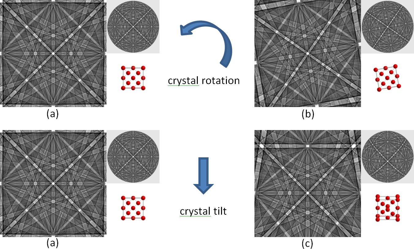
Figure 2: Effect of the rotation and tilt of single crystal silicon on the EBSD pattern: (a) Si (100), (b) crystal rotated by 10°, (c) crystal tilted by 10°. The inset placed on the right side of each picture shows the 3D spherical Kikuchi pattern and the corresponding real space views of the crystal structure. (Patterns were simulated using the trial version of Bruker’s ESPRIT DynamicS software)

Figure 3. Orientation map of a nickel sample (courtesy of Ken Mingard, NPL, Teddington)
An EBSP contains a large amount of crystallographic information from which it is possible to deduce the phase of the material under study. The space group may be determined by analysing the symmetry exhibited by the pattern. An unknown phase may be identified by a comparison of the observed symmetry with the symmetry of a list of known phases contained in a database until it is correctly identified [22].
Our EBSD research at Strathclyde is mainly focused on the development of new direct electron detectors [23]. We are using the Timepix detector [24, 25], which belongs to the CMOS hybrid pixel detectors family. It is one of the outcomes of an international collaboration (Medipix) hosted at CERN, established to provide a solution for a range of problems in X-ray and gamma-ray imaging in hostile conditions. Using the Timepix allows digital direct electron detection and energy filtering; it enables EBSPs to be acquired with reduced noise and increased contrast, and an unprecedented increase in detail is observed in the patterns (see Fig. 4).
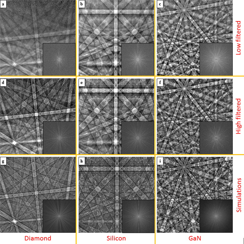
Figure 4: Experimental and simulated EBSPs from diamond (a, d, g), Si (b, e, h) and GaN (c, f, i) for an incident beam energy of 20 keV and a probe current of ~10 nA. (a–c) were acquired with a high pass energy filter of 4.6 keV, (d–f) were acquired with a high pass energy filter of 19.4 keV, and (g–i) are simulations (courtesy of Aimo Winkelmann, Bruker Nano, Berlin). The insets are 2D fast Fourier transforms of each image.
References
(The complete reference list may also be downloaded as a BibTeX database.)
[Bibtex]
@InCollection{Schwarzer2009,
Title = {Present State of Electron Backscatter Diffraction and Prospective Developments},
Author = {Schwarzer, Robert A. and Field, David P. and Adams, Brent L. and Kumar, Mukul and Schwartz, Adam J.},
Booktitle = {Electron Backscatter Diffraction in Materials Science},
Publisher = {Springer US},
Year = {2009},
Edition = {2nd},
Editor = {Schwartz, Adam J. and Kumar, Mukul and Adams, Brent L. and Field, David P.},
Pages = {1-20},
Doi = {10.1007/978-0-387-88136-2_1},
ISBN = {978-0-387-88135-5},
Language = {English},
Owner = {paul},
Timestamp = {2015.09.11}
}[Bibtex]
@Book{Goldstein2003,
Title = {Scanning Electron Microscopy and X-ray Microanalysis},
Author = {Joseph Goldstein and Dale E. Newbury and David C. Joy and Charles E. Lyman and Patrick Echlin and Eric Lifshin and Linda Sawyer and J.R. Michael},
Publisher = {Springer US},
Year = {2003},
Edition = {3rd},
Booktitle = {Scanning Electron Microscopy and X-ray Microanalysis},
Doi = {10.1007/978-0-387-88136-2_1},
ISBN = {978-0-387-88135-5},
Language = {English},
Owner = {paul},
Pages = {1-20},
Timestamp = {2015.09.11}
}[Bibtex]
@Article{Wilkinson2000JEM49,
Title = {Advances in SEM-based diffraction studies of defects and strains in semiconductors},
Author = {Wilkinson, Angus J.},
Journal = {Journal of Electron Microscopy},
Year = {2000},
Pages = {299-310},
Volume = {49},
Eprint = {http://jmicro.oxfordjournals.org/content/49/2/299.full.pdf+html},
Owner = {paul},
Timestamp = {2015.09.11},
Url = {http://jmicro.oxfordjournals.org/content/49/2/299.abstract}
}[Bibtex]
@Article{Nishikawa1928PIA4,
Title = {The diffraction of cathode rays by calcite},
Author = {Shoji Nishikawa and Seishi Kikuchi},
Journal = {Proceedings of the Imperial Academy},
Year = {1928},
Pages = {475-477},
Volume = {4},
Doi = {10.2183/pjab1912.4.475},
Owner = {paul},
Timestamp = {2015.09.11}
}[Bibtex]
@Article{Alam1954PRSA221,
Title = {High-angle {K}ikuchi patterns},
Author = {Alam, M. N. and Blackman, M. and Pashley, D. W.},
Journal = {Proceedings of the Royal Society of London A},
Year = {1954},
Pages = {224--242},
Volume = {221},
Doi = {10.1098/rspa.1954.0017},
ISSN = {0080-4630},
Owner = {paul},
Publisher = {The Royal Society},
Timestamp = {2015.09.11}
}[Bibtex]
@Article{Venables1973PM27,
Title = {Electron back-scattering patterns---A new technique for obtaining crystallographic information in the scanning electron microscope},
Author = { J. A. Venables and C. J. Harland },
Journal = {Philosophical Magazine},
Year = {1973},
Pages = {1193-1200},
Volume = {27},
Doi = {10.1080/14786437308225827},
Eprint = {
http://dx.doi.org/10.1080/14786437308225827
},
Owner = {paul},
Timestamp = {2015.09.11}
}[Bibtex]
@Article{Venables1977PM35,
Title = {Accurate microcrystallography using electron back-scattering patterns},
Author = { J. A. Venables and R. Bin-jaya },
Journal = {Philosophical Magazine},
Year = {1977},
Pages = {1317-1332},
Volume = {35},
Doi = {10.1080/14786437708232955},
Eprint = {
http://dx.doi.org/10.1080/14786437708232955
},
Owner = {paul},
Timestamp = {2015.09.11}
}[Bibtex]
@InCollection{Wright2000,
Title = {Advanced Software Capabilities for Automated {EBSD}},
Author = {Wright, Stuart I. and Field, David P. and Dingley, David J.},
Booktitle = {Electron Backscatter Diffraction in Materials Science},
Publisher = {Springer US},
Year = {2000},
Edition = {1st},
Editor = {Schwartz, AdamJ. and Kumar, Mukul and Adams, BrentL.},
Pages = {141-152},
Doi = {10.1007/978-1-4757-3205-4_13},
ISBN = {978-1-4757-3207-8},
Language = {English},
Owner = {paul},
Timestamp = {2015.09.11}
}[Bibtex]
@Article{Adams1993MTA24,
Title = {Orientation imaging: The emergence of a new microscopy},
Author = {Adams, Brent L. and Wright, Stuart I. and Kunze, Karsten},
Journal = {Metallurgical Transactions A},
Year = {1993},
Pages = {819-831},
Volume = {24},
Doi = {10.1007/BF02656503},
ISSN = {1073-5623},
Language = {English},
Owner = {paul},
Publisher = {Springer-Verlag},
Timestamp = {2015.09.11}
}[Bibtex]
@Article{KriegerLassen1992SM6,
Title = {Image processing procedures for analysis of electron back scattering patterns},
Author = {Krieger Lassen, N.C. and Juul Jensen, D. and Conradsen, K.},
Journal = {Scanning Microscopy},
Year = {1992},
Pages = {115--121},
Volume = {6},
ISSN = {0891-7035},
Owner = {paul},
Timestamp = {2015.09.11}
}[Bibtex]
@Article{KreigerLassen1998JM190,
Title = {Automatic high-precision measurements of the location and width of {K}ikuchi bands in electron backscatter diffraction patterns},
Author = {Krieger Lassen, N. C.},
Journal = {Journal of Microscopy},
Year = {1998},
Pages = {375--391},
Volume = {190},
Doi = {10.1046/j.1365-2818.1998.00330.x},
ISSN = {1365-2818},
Owner = {paul},
Publisher = {Blackwell Science Ltd, UK},
Timestamp = {2015.09.11}
}[Bibtex]
@InCollection{Day2009,
Title = {Spherical {K}ikuchi Maps and Other Rarities},
Author = {Day, Austin P.},
Booktitle = {Electron Backscatter Diffraction in Materials Science},
Publisher = {Springer US},
Year = {2009},
Edition = {2nd},
Editor = {Schwartz, Adam J. and Kumar, Mukul and Adams, Brent L. and Field, David P.},
Pages = {65-80},
Doi = {10.1007/978-0-387-88136-2_5},
ISBN = {978-0-387-88135-5},
Language = {English},
Owner = {paul},
Timestamp = {2015.09.11}
}[Bibtex]
@Article{Winkelmann2007UM107,
author = {Aimo Winkelmann and Carol Trager-Cowan and Francis Sweeney and Austin P. Day and Peter Parbrook},
title = {Many-beam dynamical simulation of electron backscatter diffraction patterns},
journal = {Ultramicroscopy },
year = {2007},
volume = {107},
pages = {414-421},
doi = {10.1016/j.ultramic.2006.10.006},
issn = {0304-3991},
owner = {paul},
timestamp = {2015.09.11}
}[Bibtex]
@InCollection{Wikelmann2009,
Title = {Dynamical Simulation of Electron Backscatter Diffraction Patterns},
Author = {Winkelmann, Aimo},
Booktitle = {Electron Backscatter Diffraction in Materials Science},
Publisher = {Springer US},
Year = {2009},
Edition = {2nd},
Editor = {Schwartz, Adam J. and Kumar, Mukul and Adams, Brent L. and Field, David P.},
Pages = {21-33},
Doi = {10.1007/978-0-387-88136-2_2},
ISBN = {978-0-387-88135-5},
Language = {English},
Owner = {paul},
Timestamp = {2015.09.11}
}[Bibtex]
@Article{Winkelmann2010NJP12,
Title = {Electron energy loss and diffraction of backscattered electrons from silicon},
Author = {Aimo Winkelmann and Koceila Aizel and Maarten Vos},
Journal = {New Journal of Physics},
Year = {2010},
Pages = {053001},
Volume = {12},
Doi = {10.1088/1367-2630/12/5/053001},
Owner = {paul},
Timestamp = {2015.09.11}
}[Bibtex]
@Article{Wells1999Scanning21,
Title = {Comparison of different models for the generation of electron backscattering patterns in the scanning electron microscope},
Author = {Wells, Oliver C.},
Journal = {Scanning},
Year = {1999},
Pages = {368--371},
Volume = {21},
Doi = {10.1002/sca.4950210602},
ISSN = {1932-8745},
Owner = {paul},
Publisher = {Wiley Periodicals, Inc.},
Timestamp = {2015.09.11}
}[Bibtex]
@Article{Matsukawa1974JPD7,
Title = {Measurements of the energy distribution of backscattered kilovolt electrons with a spherical retarding-field energy analyser},
Author = {T Matsukawa and R Shimizu and H Hashimoto},
Journal = {Journal of Physics D: Applied Physics},
Year = {1974},
Pages = {695},
Volume = {7},
Doi = {10.1088/0022-3727/7/5/306},
Owner = {paul},
Timestamp = {2015.09.11}
}[Bibtex]
@Article{Lloyd1987MinMag51,
Title = {Atomic number and crystallographic contrast images with the {SEM}: a review of backscattered electron techniques},
Author = {Lloyd, Geoffrey E},
Journal = {Mineralogical Magazine},
Year = {1987},
Pages = {3-19},
Volume = {51},
Doi = {10.1180/minmag.1987.051.359.02},
Owner = {paul},
Timestamp = {2015.09.11}
}[Bibtex]
@Article{Yubero2008PRB77,
Title = {Test of validity of the {$V$}-type approach for electron trajectories in reflection electron energy loss spectroscopy},
Author = {Yubero, F. and Pauly, N. and Dubus, A. and Tougaard, S.},
Journal = {Physical Review B},
Year = {2008},
Month = {Jun},
Pages = {245405},
Volume = {77},
Doi = {10.1103/PhysRevB.77.245405},
Issue = {24},
Numpages = {11},
Owner = {paul},
Publisher = {American Physical Society},
Timestamp = {2015.09.11}
}[Bibtex]
@Article{Winkelmann2013MM19,
Title = {Monte Carlo simulations for applications in electron backscatter diffraction},
Author = {Winkelmann,A. and Salvat-Pujol,F. and Werner,W.},
Journal = {Microscopy and Microanalysis},
Year = {2013},
Month = {8},
Pages = {738--739},
Volume = {19},
Doi = {10.1017/S1431927613005680},
ISSN = {1435-8115},
Issue = {Supplement S2},
Numpages = {2},
Owner = {paul},
Timestamp = {2015.09.11}
}[Bibtex]
@Article{Zaefferer2014AM75,
Title = {Theory and application of electron channelling contrast imaging under controlled diffraction conditions },
Author = {Stefan Zaefferer and Nahid-Nora Elhami},
Journal = {Acta Materialia },
Year = {2014},
Pages = {20 - 50},
Volume = {75},
Doi = {http://dx.doi.org/10.1016/j.actamat.2014.04.018},
ISSN = {1359-6454},
Owner = {paul},
Timestamp = {2015.09.11}
}[Bibtex]
@InCollection{Michael2000,
Title = {Phase Identification Using Electron Backscatter Diffraction in the Scanning Electron Microscope},
Author = {Michael, JosephR.},
Booktitle = {Electron Backscatter Diffraction in Materials Science},
Publisher = {Springer US},
Year = {2000},
Edition = {1st},
Editor = {Schwartz, AdamJ. and Kumar, Mukul and Adams, BrentL.},
Pages = {75-89},
Doi = {10.1007/978-1-4757-3205-4_7},
ISBN = {978-1-4757-3207-8},
Language = {English},
Owner = {paul},
Timestamp = {2015.09.11}
}[Bibtex]
@Article{Vespucci2015,
Title = {Digital direct electron imaging of energy filtered electron backscatter diffraction patterns},
Author = {S. Vespucci and A. Winkelmann and G. Naresh-Kumar and K. P. Mingard and D. Maneuski and P. R. Edwards and A. P. Day and V. O'Shea and C. Trager-Cowan},
Journal = {Accepted (22/08/2015) for publication in Physical Review B},
Year = {2015},
Owner = {paul},
Timestamp = {2015.03.24}
}[Bibtex]
@Article{Llopart2007NIMA581,
Title = {Timepix, a 65k programmable pixel readout chip for arrival time, energy and/or photon counting measurements },
Author = {X. Llopart and R. Ballabriga and M. Campbell and L. Tlustos and W. Wong},
Journal = {Nuclear Instruments and Methods in Physics Research Section A: Accelerators, Spectrometers, Detectors and Associated Equipment },
Year = {2007},
Note = {\{VCI\} 2007Proceedings of the 11th International Vienna Conference on Instrumentation },
Pages = {485 - 494},
Volume = {581},
Doi = {http://dx.doi.org/10.1016/j.nima.2007.08.079},
ISSN = {0168-9002},
Owner = {paul},
Timestamp = {2015.09.11}
}[Bibtex]
@Article{Llopart2002IEEETNS49,
Title = {Medipix2: A 64-k pixel readout chip with 55-{$\mu$}m square elements working in single photon counting mode},
Author = {Llopart, X. and Campbell, M. and Dinapoli, R. and San Segundo, D. and Pernigotti, E.},
Journal = {Nuclear Science, IEEE Transactions on},
Year = {2002},
Month = {Oct},
Pages = {2279-2283},
Volume = {49},
Doi = {10.1109/TNS.2002.803788},
ISSN = {0018-9499},
Owner = {paul},
Timestamp = {2015.09.11}
}