Electron channelling contrast Imaging (ECCI) provides rapid and non-destructive characterisation of the structural properties of materials in a scanning electron microscope (SEM). Going beyond simple topographic microscopy, ECCI is used extensively for detailed characterisation of crystalline materials ranging from metals to ceramics and semiconductors [1].
Electron channelling contrast images are produced when a sample is positioned so that a plane or planes may diffract the electrons incident on the sample. Changes in crystallographic orientation or changes in lattice constant due to local strain are revealed by changes in contrast in the channelling image constructed by monitoring the intensity of backscattered electrons as the electron beam is scanned over the sample. Extremely small changes in orientation and strain are detectable, revealing, for example, low angle tilt and rotation boundaries and atomic steps and enabling extended defects such as dislocations and stacking faults to be imaged [2, 3].
Our main application of ECCI is for the characterisation of electronic and optoelectronic devices as the reduction of defects such as threading dislocations in materials such as GaN, ZnO, SiC, and related materials is key to the optimisation of new devices. Threading dislocations act as scattering centres for light and charge carriers and give rise to nonradiative recombination and to leakage currents, severely limiting device performance [4, 5, 6].
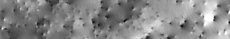
Vertical threading dislocations appear as spots with black-white (B-W) contrast; this is seen in Fig. 1, an electron channelling contrast image acquired from a nitride semiconductor thin film structure.
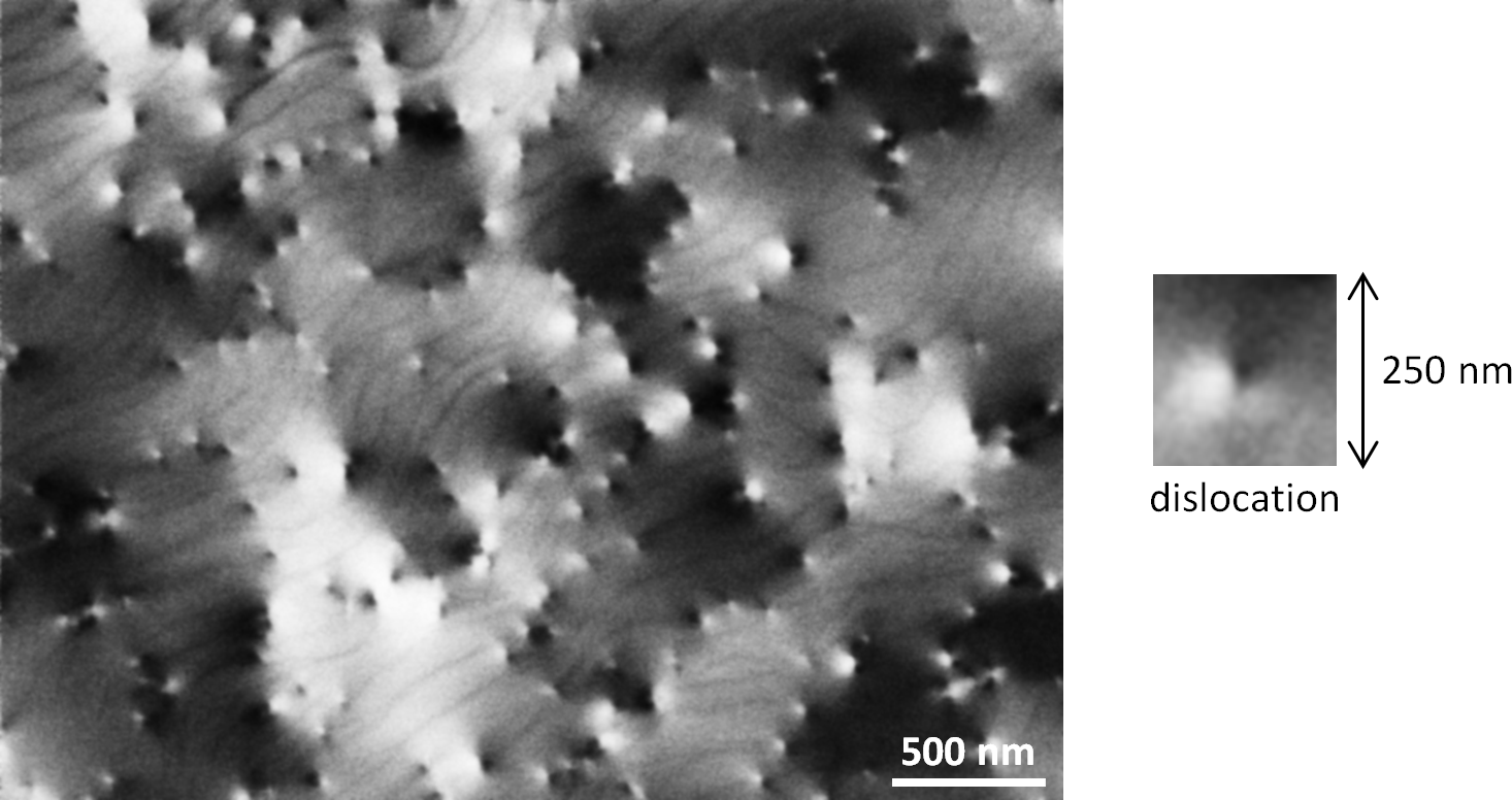
Figure 1: Electron channelling contrast image from an AlGaN/GaN high electron mobility transistor structure. The image shows dislocations (spots with black-white contrast) and atomic steps (lines). Variations in grey scale indicate variations in tilt or twist.
Fig. 2 shows an electron channelling contrast image from m-plane GaN. Stacking faults are visible as lines in the image terminated by partial dislocations.
Figure 2: Electron channelling contrast image from m-plane GaN on LiAlO2 (with a substrate offcut of 2.5° towards [010]). Some stacking faults are outlined in red.
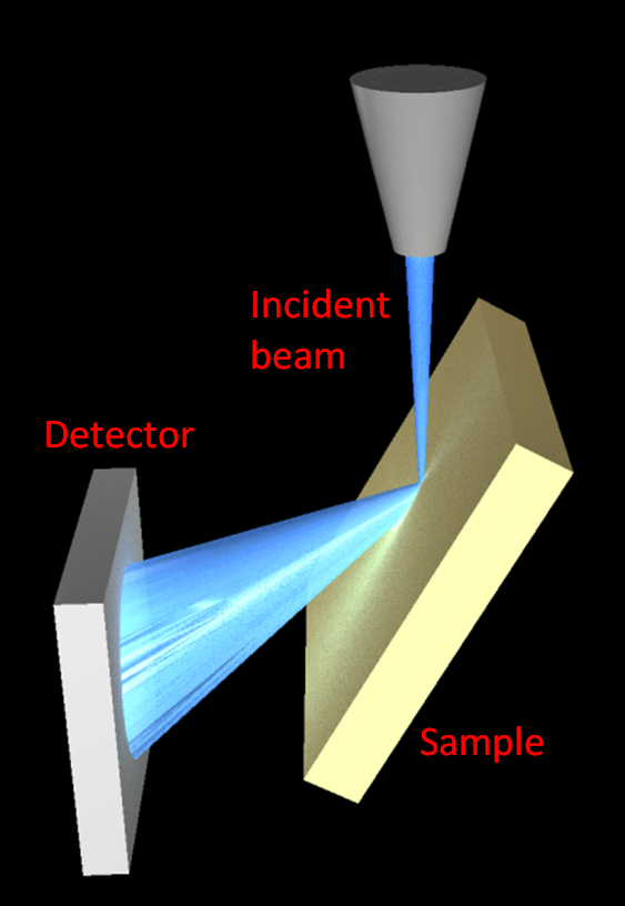
Figure 3: ECCI geometry
The conditions required to resolve individual dislocations or stacking faults in an electron channelling contrast image are quite stringent: a small (nanometres), high brightness (nanoamps or higher), low divergence (a few mrad) electron beam is required [7]. Such conditions are met in a field emission gun scanning electron microscope – we use the FEI Sirion. We use a forescatter geometry where the sample is tilted between 30° and 70° to the impinging electron beam and the backscattered electrons are detected by an electron-sensitive diode placed in front of the sample [7, 8]; see Fig. 3. It is also necessary to use a detection system that allows discrimination between electrons leaving the sample which carry channelling information and those which have been diffusely scattered by the sample. An amplifier which can offset the diffuse background signal and amplify the channelling signal is required. We a signal amplifier provided by K.E. Developments Ltd.
The acquisition of an electron channelling pattern (ECP) allows the set of planes from which the electrons are diffracted to be selected. This procedure is referred to as selecting g. An ECP is obtained when changes in the backscattered electron intensity are recorded as the angle of the incident electron beam is changed relative to the surface of a single crystal area of the sample—this is referred to as rocking the beam. When an image is acquired at low magnification, as the beam is scanned over the sample, it changes its angle with respect to the surface of the sample (in our case by around 2.5°) allowing an ECP to be obtained. When the beam is rocked over the sample, different planes of the crystal satisfy the Bragg condition, giving rise to the appearance of overlapping bands of bright and dark lines (Kikuchi lines [9]) superimposed on the image of the sample; this is the ECP, as seen in Fig. 4. The ECP is a 2-D projection of the crystal lattice. Tilting the sample moves the ECP up and down on the viewing screen and rotating the sample moves the ECP from left to right. The pattern centre (PC) of the ECP corresponds to the plane(s) from which the incident electrons are diffracted.
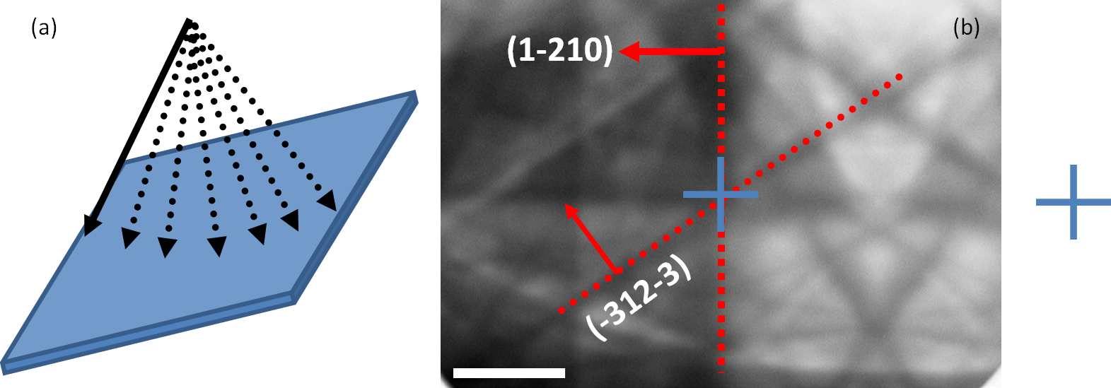
Figure 4: (a) Illustrating beam rocking (b) ECP from a GaN thin film
Combining ECCI with other techniques in the SEM such as energy dispersive X-ray mapping or cathodoluminescence mapping allows the correlation of structural and compositional properties, or structural and luminescence properties of materials. For example Fig. 5 below shows an electron channelling contrast image and a hyperspectral cathodoluminescence intensity map of the near band edge emission (NBE) from approximately the same region of a Al0.8Ga0.2N:Si thin film (~ 1.5 µm) grown on epitaxially laterally overgrown AlN on a patterned AlN/sapphire template. The NBE has a peak at around 5.3 eV for this sample.
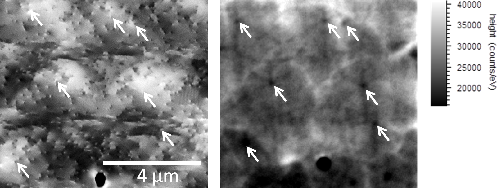
Figure 5: (a) Electron channelling contrast image (b) Cathodoluminescence NBE intensity image. Arrows indicate threading dislocations with a screw component which appear as dark spots in the cathodoluminescence image.
From the images presented in Fig. 5 above we can conclude that different crystalline domains are formed due to spiral growth around dislocations with a screw component which act as nonradiative recombination centres for NBE emission [10].
References
(The complete reference list may also be downloaded as a BibTeX database.)
[Bibtex]
@Article{Wilkinson1997Micron28,
author = {Angus J. Wilkinson and Peter B. Hirsch},
title = {Electron diffraction based techniques in scanning electron microscopy of bulk materials },
journal = {Micron},
year = {1997},
volume = {28},
pages = {279 - 308},
doi = {10.1016/S0968-4328(97)00032-2},
issn = {0968-4328},
keywords = {scanning electron microscopy},
owner = {paul},
timestamp = {2015.09.11}
}[Bibtex]
@Article{Naresh-Kumar2012PRL108,
Title = {Rapid nondestructive analysis of threading dislocations in wurtzite materials using the scanning electron microscope},
Author = {Naresh-Kumar, G. and Hourahine, B. and Edwards, P. R. and Day, A. P. and Winkelmann, A. and Wilkinson, A. J. and Parbrook, P. J. and England, G. and Trager-Cowan, C.},
Journal = {Physical Review Letters},
Year = {2012},
Pages = {135503},
Volume = {108},
Doi = {10.1103/PhysRevLett.108.135503},
Owner = {Paul},
Timestamp = {2012.04.27}
}[Bibtex]
@Article{Naresh-Kumar2013APL102,
Title = {Electron channeling contrast imaging studies of non-polar nitrides using a scanning electron microscope},
Author = {Naresh-Kumar, G. and Mauder, C. and Wang, K. R. and Kraeusel, S. and Bruckbauer, J. and Edwards, P. R. and Hourahine, B. and Kalisch, H. and Vescan, A. and Giesen, C. and Heuken, M. and Trampert, A. and Day, A. P. and Trager-Cowan, C.},
Journal = {Applied Physics Letters},
Year = {2013},
Pages = {142103},
Volume = {102},
Doi = {10.1063/1.4801469},
Owner = {Paul},
Timestamp = {2013.03.27}
}[Bibtex]
@Article{Look1999PRL82,
Title = {Dislocation Scattering in {GaN}},
Author = {Look, D. C. and Sizelove, J. R.},
Journal = {Physical Review Letters},
Year = {1999},
Month = {Feb},
Pages = {1237--1240},
Volume = {82},
Doi = {10.1103/PhysRevLett.82.1237},
Issue = {6},
Numpages = {0},
Owner = {paul},
Publisher = {American Physical Society},
Timestamp = {2015.09.11}
}[Bibtex]
@Article{Wu1996JAP80,
Title = {Defect structure of metal-organic chemical vapor deposition-grown epitaxial (0001) GaN/Al₂O₃},
Author = {Wu, X. H. and Brown, L. M. and Kapolnek, D. and Keller, S. and Keller, B. and DenBaars, S. P. and Speck, J. S.},
Journal = {Journal of Applied Physics},
Year = {1996},
Pages = {3228-3237},
Volume = {80},
Doi = {http://dx.doi.org/10.1063/1.363264},
Owner = {paul},
Timestamp = {2015.09.11}
}[Bibtex]
@Article{Liu2007JAC40,
author = {Liu, W.-R. and Hsieh, W. F. and Hsu, C.-H. and Liang, Keng S. and Chien, F. S.-S.},
title = {Threading dislocations in domain-matching epitaxial films of {ZnO}},
journal = {Journal of Applied Crystallography},
year = {2007},
volume = {40},
pages = {924--930},
month = {Oct},
doi = {10.1107/S0021889807033997},
keywords = {X-ray diffraction, epitaxial film, ZnO, dislocation},
owner = {paul},
timestamp = {2015.09.11}
}[Bibtex]
@Article{Trager-Cowan2007PRB75,
Title = {Electron backscatter diffraction and electron channeling contrast imaging of tilt and dislocations in nitride thin films},
Author = {Trager-Cowan, C. and Sweeney, F. and Trimby, P. W. and Day, A. P. and Gholinia, A. and Schmidt, N.-H. and Parbrook, P. J. and Wilkinson, A. J. and Watson, I. M.},
Journal = {Physical Review B},
Year = {2007},
Month = {Feb},
Pages = {085301},
Volume = {75},
Doi = {10.1103/PhysRevB.75.085301},
Issue = {8},
Numpages = {8},
Owner = {paul},
Publisher = {American Physical Society},
Timestamp = {2015.09.11}
}[Bibtex]
@Article{Simkin1999UM77,
Title = {An experimentally convenient configuration for electron channeling contrast imaging},
Author = {Simkin, BA and Crimp, MA},
Journal = {Ultramicroscopy},
Year = {1999},
Pages = {65--75},
Volume = {77},
Doi = {10.1016/S0304-3991(99)00009-1},
Owner = {paul},
Publisher = {Elsevier},
Timestamp = {2015.09.11}
}[Bibtex]
@InCollection{Williams2009,
Title = {Kikuchi Diffraction},
Author = {Williams, David B. and Carter, C. Barry},
Booktitle = {Transmission Electron Microscopy},
Publisher = {Springer US},
Year = {2009},
Pages = {311-322},
Doi = {10.1007/978-0-387-76501-3_19},
ISBN = {978-0-387-76500-6},
Language = {English},
Owner = {paul},
Timestamp = {2015.09.11}
}![[pdf]](https://gan-sem.phys.strath.ac.uk/wp-content/plugins/papercite/img/pdf.png)
[Bibtex]
@Article{Kusch2015APL107,
Title = {Spatial clustering of defect luminescence centers in {Si}-doped low resistivity {Al₀.₈₂Ga₀.₁₈N}},
Author = {G. Kusch and M. Nouf-Allehiani and F. Mehnke and C. Kuhn and P. R. Edwards and T. Wernicke and A. Knauer and V. Kueller and M. Weyers and G. Naresh-Kumar and M. Kneissl and C. Trager-Cowan and R. W. Martin},
Journal = {Applied Physics Letters},
Year = {2015},
Pages = {072103},
Volume = {107},
Doi = {10.1063/1.4928667},
Owner = {paul},
Timestamp = {2015.07.14}
}